Transistor Advances - From Planar MOSFETs to CFET Stacks
“No exponential is forever, but we can delay ‘forever’.” — Gordon Moore
For many of us in network engineering, it’s easy to overlook the semiconductor technology that makes our work possible. While we are focused on packet processing details and how network protocols work, semiconductor engineering is what drives the continuous improvement of networking hardware.
When we see new silicon offering higher bandwidth or lower latency, it’s easy to overlook the underlying innovations that make those gains possible. By understanding these breakthroughs, we can better appreciate the progress—and the trade-offs—that come with modern transistor scaling.
In this overview, I will discuss transistor technology’s progression, the reasons Dennard scaling hit a wall, and possible steps beyond FinFETs and 3D stacking.
Moore’s Law
A natural starting point is Moore’s Law, famously associated with Gordon Moore, co-founder of Intel. Moore predicted in his seminal paper, “Cramming more components onto integrated circuits”, that the number of transistors on integrated circuits would double roughly every two years—largely propelled by continuous advancements in lithography.
Over the years, semiconductor industry followed Moore’s Law based on ideas from a 1974 paper by R. Dennard. Each new node typically cuts transistor area by around 50%, lowers cost by about 30%, reduces power by 20%, and boosts performance by 25%. Together, these factors—Power, Performance, Area, and Cost (PPAC)—determine whether a node is worth pursuing. However, It’s important to remember that Moore’s Law is an economic principle, not a fundamental law of physics: transistor scaling endures only as long as the advantages of shrinking transistors outweigh the rising complexity and cost of making them.
Transistor scaling strategies have shifted dramatically over the years. In the 1990s, Dennard’s constant field scaling shrank all dimensions—gate length, operating voltage, gate oxide thickness, and so forth—by the same factor ( $\frac{1}{k}$). This preserved uniform electric fields and kept power density in check while boosting performance. Since both dimensions and voltage dropped by ( $\frac{1}{k}$), transistors ran faster by the same factor without raising power consumption.
As dimensions pushed even smaller, however, constant field scaling hit roadblocks such as threshold voltage constraints and rising leakage currents. This led to the modern “general scaling” approach, which optimizes power, performance, and area independently, making trade-offs wherever necessary.
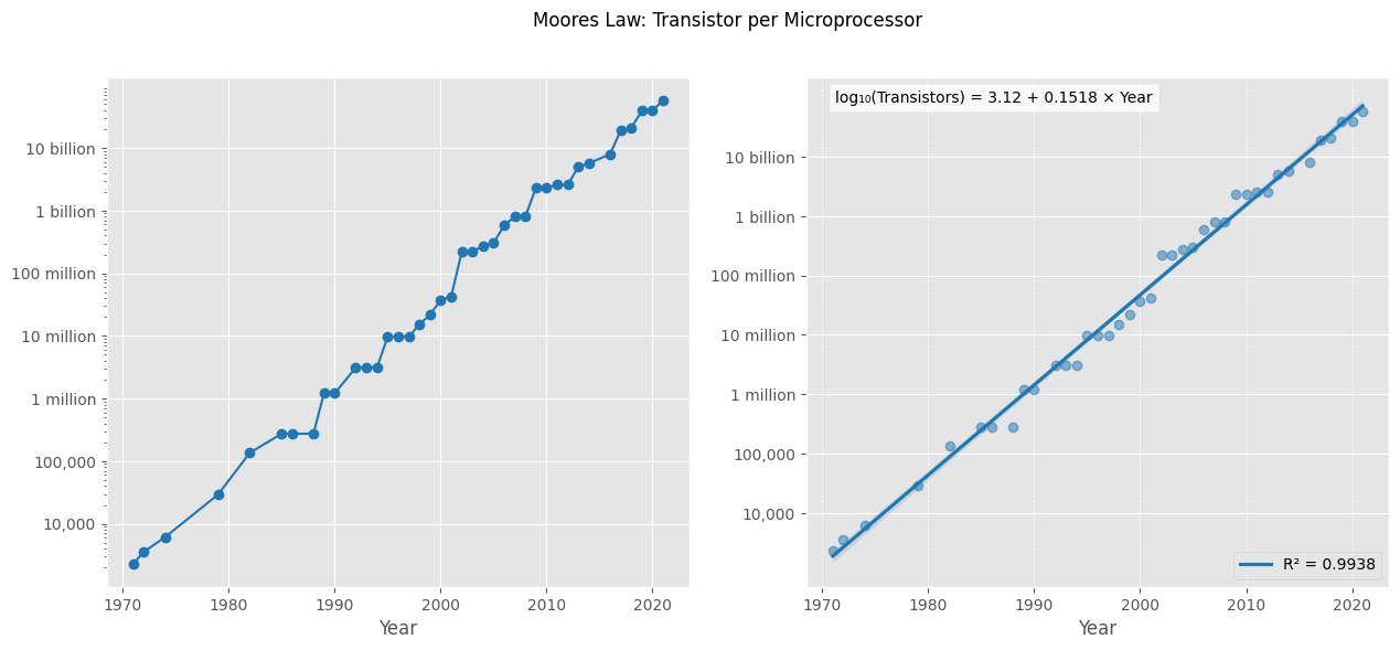
The graph demonstrates Moore’s Law in action through actual transistor counts from 1970 to 2020.
Ref: ourworldindata: Transistor per Microprocessor
Performing a linear regression on the data, I got a growth coefficient of $0.1518$ which translates to roughly of 42% annual growth ($10^{0.1518} \approx 1.421$). Over two years, this compounds to $~2.018$ ($(1+0.421)^2 \approx 2.018$) increase, which is remarkably close to Moore’s predicted doubling.
Modern Process Nodes: Marketing vs. Reality
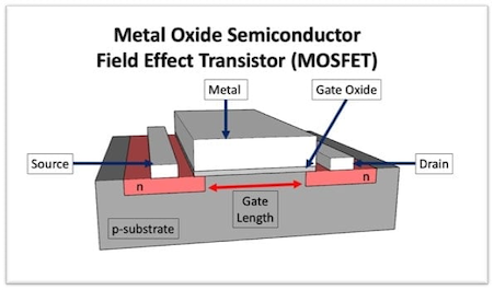
At a high level, transistor is a switch. Below is a schematic of a planar transistor which shows the source, drain and the gate which controls the flow of current between source and drain. The gate length is the distance between source and drain.
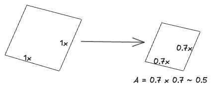
Transistor process nodes used to reflect the true physical size of the gate length. Every two years, the gate length would shrink by about 30% (from 1 to 0.7x). This shrinkage cut the die area in half $(\text{since }0.7 \times 0.7 = 0.5)$, allowing the transistor count to double in the same area.
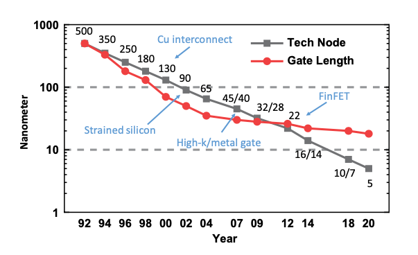
The figure below illustrates silicon logic process scaling trend, specifically focusing on gate length and technology node names. Historically, the technology node aligned with the actual gate length of logic transistors. This meant that the technology node name represented the gate length.
Ref:Semiconductor Memory Devices and Circuits
However, as technology advanced, gate lengths were aggressively scaled down to sizes much smaller than their corresponding technology nodes. Subsequently, gate length reductions slowed due to limitations imposed by short channel effects, resulting in slow down in gate length reduction for 22 nm and beyond.
Even though gate lengths stopped shrinking at the same pace, the semiconductor industry continued labeling each new node with the “0.7x rule,” using names like 22 nm, 14 nm, and 10 nm, and more recently 3 nm and 2 nm. Today, these labels no longer correspond to the true transistor gate length; they’ve largely become marketing terms rather than accurate measurements of transistor features.
Key Transistor Parameters and Basic Operation
It’s essential to understand a few fundamental parameters when examining transistor behavior.
Voltage
Threshold Voltage ($V_{th}$) is the minimum gate-to-source voltage ($V_{gs}$) needed to switch a transistor “on”. Below this level, the transistor remains effectively off and blocks current. You can think this like a door latch- you must push beyond a certain point to open the door and let current flow.
Supply Voltage ($V_{DD}$) is the power or operating voltage provided to the circuit. It serves as the “high” voltage level, driving the gate strongly enough to fully switch the transistor on.
Current
On Current ($I_{on}$) This is the current flowing through a transistor when it’s fully on (i.e., when $V_{gs}$ is well above $V_{th}$). A higher $I_{on}$ implies faster switching, since charge can move more quickly. However, it also increases power consumption when the device is active, due to the larger current flow.
Off Current or Leakage Current($I_{off}$) is the (ideally negligible) current that flows when the transistor is turned off ($V_{gs}$ is below $V_{th}$). In reality, a small amount of leakage current still flows for two main reasons:
- Subthreshold Leakage: Current that flows even when $V_{gs}$ is below $V_{th}$, which increases exponentially as $V_{th}$ decreases.
- Gate Oxide Leakage: Current that sneaks through the gate oxide layer. As transistors shrink, the oxide layer gets thinner, making this form of leakage more pronounced.
Capacitance
Gate Capacitance ($C_{gate}$) originates from the thin dielectric layer between a transistor’s gate and its channel, effectively creating a small capacitor that must charge and discharge during every switching event. As transistor dimensions scale down, the gate area shrinks, which reduces $C_{gate}$ and can improve performance. However, when the dielectric becomes extremely thin, gate oxide leakage rises, posing new challenges.
Diffusion/Parasitic Capacitances ($C_{diff}$) are caused by the p-n junctions at the source/drain regions and any other incidental (“parasitic”) capacitances where conductive elements are in close proximity. Although modern transistor scaling has substantially lowered $C_{gate}$, these parasitic effects have become a larger fraction of overall device capacitance and do not always scale down as smoothly.
Interconnect Capacitances ($C_{wire}$) Metal wires themselves can act as capacitors relative to each other and to ground. As chip layouts become denser, these interconnect capacitances increasingly dominate both delay and power consumption. In fact, in many high-performance circuits, $C_{wire}$ can exceed all transistor-level capacitances combined.
Total Load Capacitance($C_{load}$) represents the combined effect of gate, diffusion/parasitic, and interconnect capacitances. Each time a transistor switches, it must charge or discharge every capacitance hanging on its output. Both the switching speed and power consumption hinge on this total load capacitance, working in tandem with the transistor’s on-current ($I_{on}$).
Transistor Delay and Power
Transistor Delay ($\frac{CV}{I}$) When a transistor switches, it charges or discharges a total load capacitance $C$ via its drive current $I$. The delay ($\frac{CV}{I}$) approximates how long this process takes. You can picture the capacitance as a “bucket” of charge, the voltage V as the “pressure” pushing charge in or out, and the current $I$ as the “flow rate.” Each switching event moves a charge of $Q = CV$. A larger capacitance (“bigger bucket”) or higher voltage (“more pressure”) increases the total charge that must be transferred, prolonging the delay. In contrast, a higher current fills or empties the bucket faster, reducing delay.
This charging time dictates how quickly a system can be clocked. A lower delay means faster switching, allowing higher operating frequencies.
Dynamic Power Dynamic power is the energy consumed whenever transistors toggle between states. Each switching event charges or discharges various load capacitances, incurring an energy cost proportional to both the capacitance and the square of the supply voltage:
\[P_{\text{dyn}} = \alpha \times C \times f \times V^{2}_{DD}\]where:
- $\alpha$ is the activity factor (fraction of gates switching each clock cycle).
- $C$ is the total switching capacitance (sum of gate, diffusion, interconnect, etc. for all nodes).
- $f$ is the clock frequency.
- $V^{2}_{DD}$ is square the operating voltage.
A higher switching frequency or an increased supply voltage translates into more energy used to charge and discharge these capacitances, thus raising dynamic power.
Static Power Static power is the energy consumed even when the circuit is idle—meaning no active switching is taking place. It mainly stems from leakage currents passing through transistors that, under ideal conditions, would remain “off.”
\[P_{static} = V_{DD} \times I_{off}\]where:
- $I_{off}$ is the leakage current that flows through the transistor when it’s supposed to be “off.”
Energy $CV^2$
Each time a node switches from 0 to V or back again, a certain amount of charge must be transferred, incurring an energy cost of ($\frac{1}{2}CV^2$). It’s common to simplify this to $CV^2$ in broader power discussions. This energy isn’t stored long-term; rather, it’s released as heat within the transistor channel during each switching event.
Dennard Scaling: The Golden Age of Power Efficiency
Dennard scaling, named after Robert Dennard, emerged from his influential 1974 paper showing how the power density of MOSFET transistors could stay roughly constant as dimensions shrank. Put simply, if you shrink a transistor’s length, width, and oxide thickness by a factor k, you also reduce the supply voltage and operating voltage by k. Under these ideal conditions, the power per unit area remains nearly the same, even as clock frequencies and transistor densities climb.
This principle is captured by the dynamic power equation:
\[P_{\text{dyn}} = \alpha \times C \times f \times V^{2}_{DD}\]By scaling both voltage and capacitance by k, you can, in theory, boost the switching frequency without raising total power consumption. Historically, this allowed clock frequencies to rise with each new process node.
You can see in the plot below how the frequency grew without Power increase until the Dennard scaling broke down. The marriage of Moore’s law and Dennard scaling is considered as the golden era.
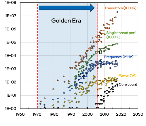
Ref:Moore’s Law and Dennard scaling
Why Dennard Scaling Broke Down
Dennard’s scaling principle hinges on the assumption that the transistor threshold voltage ($V_{th}$) would shrink in tandem with the operating voltage, thereby boosting both performance and power efficiency. However, the original 1974 model largely ignored the impact of sub-threshold leakage on total chip power—a negligible factor in the 1970s.
After decades of aggressive scaling, that assumption fell apart. As $V_{th}$ was driven lower, sub-threshold leakage grew by orders of magnitude. This massive increase in leakage prevented further reductions in $V_{th}$, effectively capping how much we can lower the supply voltage.
A second stumbling block is gate oxide thickness scaling, which for decades provided major gains. By the 90nm/65nm technology generation, Intel was deploying a $SiO_2$ gate dielectric only 1.2 nm thick—about five atomic layers of silicon. This is near the physical limit of $SiO_2$, and direct tunneling through such thin oxide layers significantly amplifies power consumption.
Additionally, Dennard’s law assumed continuous increases in channel doping concentration to preserve $V_{th}$ as channel lengths shrank. This assumption met two key hurdles:
- Heavier doping reduces carrier mobility, damaging performance due to greater impurity scattering.
- Source and drain junction leakage surges from direct band-to-band tunneling.
All these limitations collectively ended Dennard scaling and compelled the industry to seek new avenues for further progress.
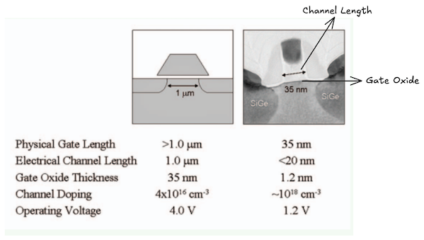
Below is a comparison of the Transistor structure from Dennard’s 1974 paper with Intel’s 65nm generation in 2005. You can see the gate length decreased from $\approx 1\mu\text{m}$ to $35nm$ and gate oxide thickness from $35nm$ to $1.2nm$.
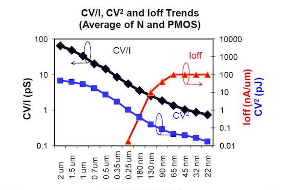
In the below plot, you can see how transistor delay ($\frac{CV}{I}$), energy consumed ($CV^2$) and leakage current ($I_{OFF}$) evolve as the process node advances. While both delay and energy consumed is decreasing with new process nodes, leakage current ($I_{OFF}$) climbs dramatically at 130nm node–largely due to shorter channel lengths and thinner gate oxides.
Ref:CMOS Scaling
Evolution of Transistor Technology
Planar MOSFET: The Early Workhorse
Traditional MOSFET scaling was highly effective until the 130 nm node in the early 2000s. At that point, the $SiO_{2}$ gate oxide reached about 1.5 nm in thickness, causing a surge in electron tunneling and a corresponding rise in leakage current. This issue signaled the practical limit of traditional scaling, prompting researchers to explore new materials and transistor structures.
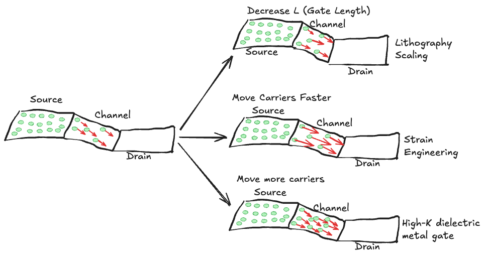
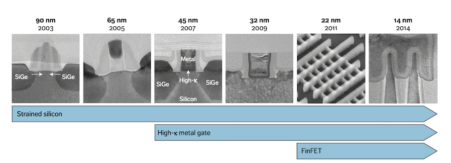
One of the key breakthroughs came in 2003, when Intel introduced strained silicon transistors at the 90 nm node. Tensile strain applied to the NMOS channel via a high-stress film enhanced electron mobility, boosting on-current. Simultaneously, compressive strain in PMOS devices was achieved by replacing source and drain regions with epitaxially grown SiGe to improve hole mobility. Together, these techniques elevated transistor performance without requiring further thinning of the ${SiO_2}$ layer.
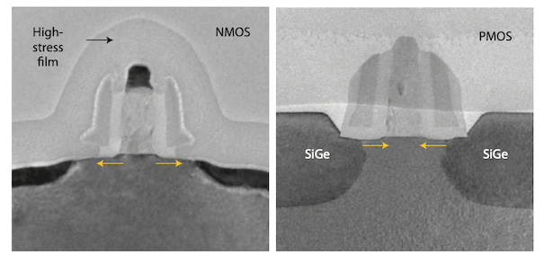
Ref: IEDM 2003 N90 Strain Engineering
The next major leap addressed the gate dielectric. In 2007, Intel adopted high-k metal gate transistors at the 45nm node, replacing the traditional ${SiO_2}$ dielectric with a hafnium-based high-k material—thereby reducing gate leakage and enhancing drive currents. In parallel, metal electrodes supplanted doped polysilicon gates to fine-tune threshold voltages in NMOS and PMOS devices. This combination of high-k dielectrics and metal gate electrodes transformed transistor design, lowering leakage current and enhancing device performance.
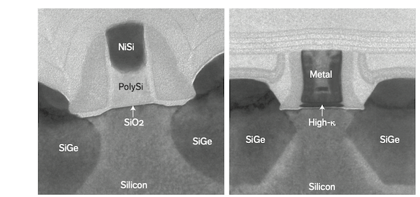
Ref: Implementation of high-k dielectric and metal electrode in 45 nm technology
FinFET: Moving to 3D
A major step forward came with the introduction of FinFET (trigate) transistors at the 22-nm in 2011. Traditional planar MOSFETs could be scaled down to a gate length of about 32 nm while still maintaining good performance, density, and low off-state leakage. However, scaling below 32-25 nm became increasingly difficult without compromising either performance or leakage. The solution was to move away from planar designs to a three-dimensional FinFET structure, where the gate electrode surrounds a tall, narrow silicon fin.
The wells, sources, and drains were lifted onto this “fin,” with the gate wrapping around the well regions. Transistors could be made of multiple fins with a single gate on top.
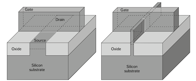
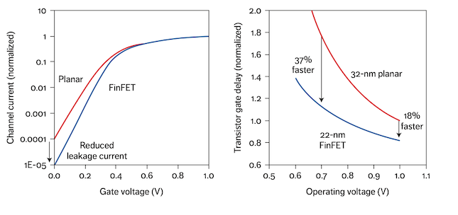
This structure offers much better electrostatic control of the channel, which in turn leads to a steeper sub-threshold slope. We can see in the plot below(left), the FinFET curve (blue) lies below the planar curve (red). This indicates that FinFETs have lower off-state leakage current at small gate voltages. Moreover, the steeper transition in the FinFET current as gate voltage rises reflects the stronger electrostatic control that FinFET technology provides.
FinFETs offer two key advantages over planar transistors: they produce less off-state leakage and enable a lower threshold voltage, thereby boosting performance at reduced operating voltages. Running circuits at lower voltages is crucial for curbing active power consumption. In the plot below(right), the FinFET curve stays beneath the planar curve at every voltage level, demonstrating that FinFETs’ have faster switching speed (lower delay) across the full voltage range.
The figure below shows how, once traditional MOSFET scaling lost momentum in the early 2000s, new technologies—strained silicon, high-k metal gate, and FinFETs were introduced.
Ref: Advance Device Concepts for 7nm Node and Beyond
By adopting FinFETs, it became possible to operate at lower voltages yet maintain lower leakage, thereby cutting power consumption by roughly 50% at the same performance level compared to the previous planar generation. FinFETs also switch faster, yielding a 37% performance boost. In addition, because current flows on both vertical sides of the “fin,” each transistor drives more current per unit area than a planar device, which conducts only along one surface.
FinFet Geometry: Pitch, Height, and Scaling
Below is a depiction of the core geometric parameters in a FinFET transistor, noting that a single transistor can include multiple fins:
Fin Thickness(Fth): The width of each fin.
Fin Height(FH): The vertical dimension of the fin. Taller fins effectively increase the channel width, allowing the gate to enclose more area and resulting in higher drive current.
Fin Pitch(FP):The distance between adjacent fins. A smaller fin pitch allows more transistors to be packed into the same area.
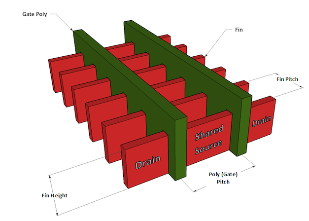
Metal Pitch (MP): The center-to-center distance between neighboring metal interconnect lines on a given routing layer.
- Smaller pitch: Increases wiring density, but elevates wire resistance and can raise reliability concerns.
- Larger pitch: Eases manufacturing and lowers wire resistance, but reduces routing density.
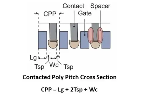
Poly (Gate) Pitch/ Contacted Gate Pitch(CGP)/Contacted Poly Pitch(CPP): It is the horizontal distance from the center of a transistor gate to the corresponding adjacent transistor gate. A common way to express CGP is:
$\text{CGP (CPP)} = L_\text{g} + 2 \times T_\text{sp} + W_\text{c}$
where:
- $L_\text{g}$ = Gate length (the critical dimension of the transistor channel)
- $T_\text{sp}$ = Spacer thickness (material separating the gate from other regions)
- $W_\text{c}$ = Contact width (size of the gate’s contact)
Ref: IEDM 2022 – TSMC 3nm
Logic chips are built from standard cell libraries, where each standard CMOS cell typically contains both a PMOS and an NMOS transistor. In a FinFET design, each transistor can include multiple fins. The illustration here depicts a standard cell with both PMOS and NMOS transistors. Standard cells are characterized by three main dimensions: CGP, FP and MP.
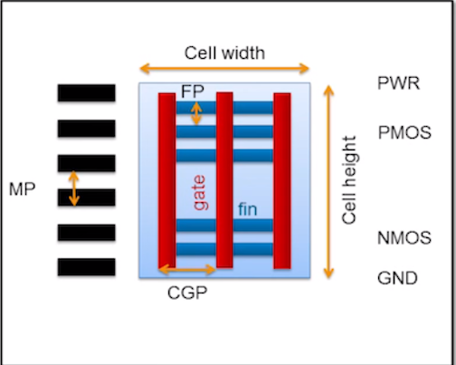
Below are dimensions details for various TSMC nodes.
| Node | $CPP(nm)$ | $L_{g}(nm)$ | $T_{sp}(nm)$ | $W_{c}(nm)$ |
|---|---|---|---|---|
| 16nm | 90 | 30 | 18 | 24 |
| 10nm | 66 | 23 | 12.5 | 18 |
| 7nm | 54 | 21 | 10 | 13 |
| 5nm | 51 | 19 | 9.5 | 13 |
Ref: IEDM 2022 – TSMC 3nm
In early FinFET designs, fins were relatively short and tapered. In the next generation, however, they evolved into taller, thinner, more rectangular structures. Taller fins increase the effective channel width (Weff), given by Weff = 2Fh + Fth, where Fh is the fin height and Fth is the fin thickness. Increasing Weff increases drive current for heavily loaded circuits but excessively tall fins waste active power.
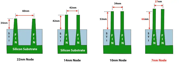
Finfet fin dimensions for various nodes.
| 22nm | 14nm | 10nm | 7nm | |
|---|---|---|---|---|
| Channel Length | 25 | 22 | 19 | 16 |
| Fin Width | 10 | 9 | 8 | 7 |
| Fin height | 34 | 42 | 53 | 66 |
Scaling Strategies in the FinFET Era: Feature Shrink vs. Depopulation
With the advent of FinFETs, transistor scaling took on a new dimension. While the traditional approach of shrinking every component of a transistor still exists, a new “depopulation” strategy emerged in which each transistor is formed with fewer features overall. These two paths—feature shrink and depopulation—are both employed in modern semiconductor processes, but practical manufacturing obstacles and physics constraints have made the traditional path of feature shrink less dominant. As a result, depopulation has become the dominant avenue for increasing transistor density in the FinFET era.
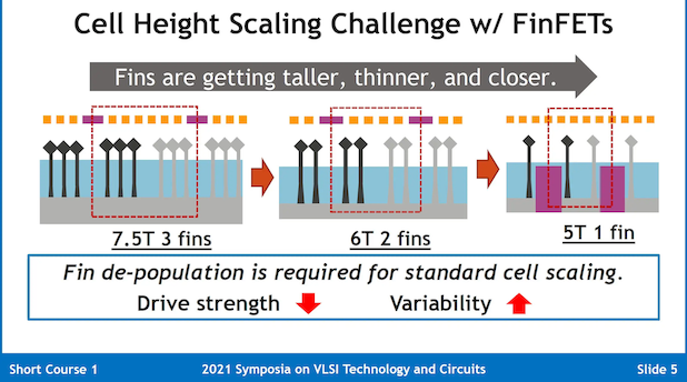
Ref: FinFET scaling
Transistors themselves are typically arranged in arrays. For instance, imagine a FinFET array that spans eight fins in width and three gates in height, with each transistor defined by the intersection of a single gate and four fins. Such an arrangement might house six transistors (2x3).
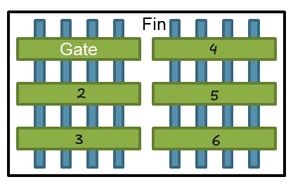
To double the transistor count in the same footprint, one could either shrink the dimensions to accommodate 12 fins and four gates or “depopulate” by assigning just two fins to each gate, keeping feature sizes constant. Although both strategies are employed, reducing fin count (i.e., depopulation) now accounts for most density gains.

Ref:Feature shrink
Naturally, using fewer fins lowers the total gate-well surface area, which complicates the power–performance balance. The challenge becomes enhancing each fin’s performance so that the overall transistor can still meet or exceed the required power and speed targets. One straightforward solution is to make fins taller, recovering some lost channel width. However, taller fins are more fragile, more susceptible to etch defects, and require meticulous attention to sidewall straightness. Furthermore, gate fill using metal becomes more difficult at higher aspect ratios, prompting engineers to solve new issues in deposition uniformity.
Gate-All-Around (GAA) FETs
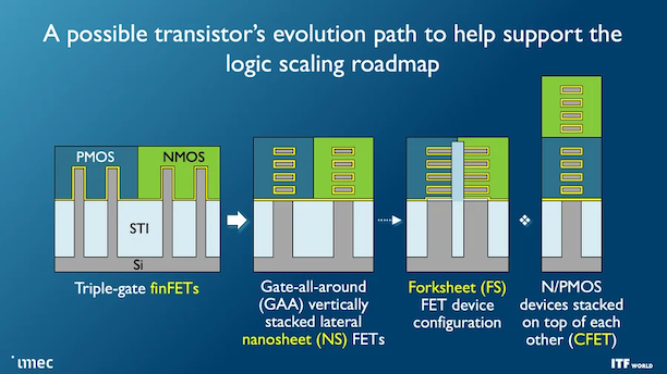
Gate-all-around (GAA) devices are widely regarded as the natural successor to FinFETs for technology nodes at or below 3 nm. The essential challenge with continued FinFET scaling is maintaining stringent electrostatic control—particularly evident in the subthreshold swing—which becomes more difficult as fin widths shrink. GAA technology addresses this by fully surrounding the channel with the gate, thereby improving control over leakage currents and threshold-voltage variations. The subthreshold swing improves at shorter gate lengths when moving from FinFET to GAA (also referred to as nanosheet or nanowire devices).
We can see the geometric differences among FinFET, nanowire, and nanosheet devices.
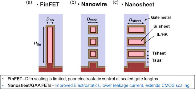
Ref: Comparison of FinFet, Nanowire and Nanosheet
By placing the gate on all sides of the channel, GAA transistors minimize parasitic short-channel effects and enable higher performance and lower power consumption. At the same time, however, they demand more complex fabrication steps, tighter layout constraints, and innovations in spacer and contact engineering, as well as potential changes to standard-cell design. Overall, GAA represents a key evolution in transistor architecture, pushing beyond the limits of FinFET scaling to continue delivering improvements in performance, leakage control, and power efficiency.
TSMC 2NM technology will be based on Gate All Around transistors TSMC Details Its High-End “2nm Process”.
CFET: Stacking pMOS and nMOS for True 3D
CFET (Complementary FET) is a three-dimensional device architecture that stacks pMOS and nMOS transistors on top of each other around a shared gate. The motivation behind CFET arises from the need to sustain Moore’s law scaling beyond the limitations of conventional 2D layouts. As standard FinFETs and even nanosheet-based FETs push toward smaller nodes, routing congestion and parasitic elements in the interconnects become significant bottlenecks. CFET tackles this problem by stacking devices vertically, thereby greatly reducing the area required by standard cells and SRAM blocks. CFET has a potential to get 1.5 to 2x density improvements for standard cells as compared to the conventional CMOS architecture.
Ref: Schematic representation of a CFET device.
We can see that the pMOS and nMOS structures are literally placed on top of each other with a common gate (G). Their respective sources (Sp for pMOS and Sn for nMOS) and drains (Dp for pMOS and Dn for nMOS) are folded in such a way that interconnects can be routed more compactly. Since both pMOS and nMOS devices share the same gate, there is an inherent complementary nature that benefits overall circuit performance. Additionally, CFET can fit neatly into gate-all-around (GAA) flows: once the bottom device is formed up to the source/drain level, the top device can then be fabricated over it, with proper sealing steps to isolate one tier while processing the other.
One of the biggest advantages of CFET, besides layout area reduction, is its ability to ease some of the parasitic effects that hamper 2D scaling. By exploiting a true three-dimensional structure, CFET addresses routing overheads in the “x-y” plane. However, realizing CFET in a manufacturing flow does introduce complexity. The top device must tolerate a low-thermal-budget process to avoid degrading the bottom device, and the entire stack requires reliable isolation layers.
Below is IMEC’s prediction of potential roadmap extension
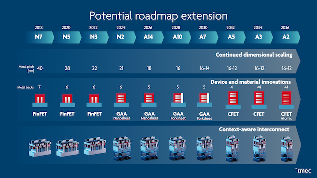
Ref: Imec’s prediction of potential roadmap extension
Conclusion
We began with planar MOSFETs, moved on to FinFETs, then saw the rise of GAA and CFET—each step addressing new challenges and propelling transistor design forward. By understanding this progression, we gain a clearer view of what powers modern chips at 5 nm, 3 nm, and beyond, like Broadcom’s Tomahawk 5 on TSMC’s 5 nm process. Now, when we hear about the latest “nm” node or a new networking silicon release, we can connect those claims to the real transistor-level innovations making them possible.
References
- Cramming More Components onto Integrated Circuits
- The number of transistors per microprocessor
- CMOS Scaling
- 42 Years of Microprocessor Trend Data
- Semiconductor Memory Devices and Circuits
- imec chip scaling roadmap
- Review of nanosheet metrology opportunities for technology readiness
- Meet the Forksheet
- 2021 Symposium on VLSI Technology and Circuits
- Introduction to GAAFET: The Next Big Phase of Computer Chip Manufacturing
- Critical Process features Enabling Aggressive Contacted Gate Pitch Scaling for 3nm CMOS Technology and Beyond
- FinFet Technology and Beyond
- Advance Device Concepts for 7nm Node and Beyond
- The Incredible Shrinking Transistor
- 2D to 3D MOS Technology Evolution for Circuit Designers